Experiments in nano manufacturing
There’s Plenty of Room at the Bottom. —Richard Feynman
With the recent demise of Milly’s electron emitter, I attempted to make a new one. Much to my surprise, it worked.
Turns out making small things is harder than it might seem.
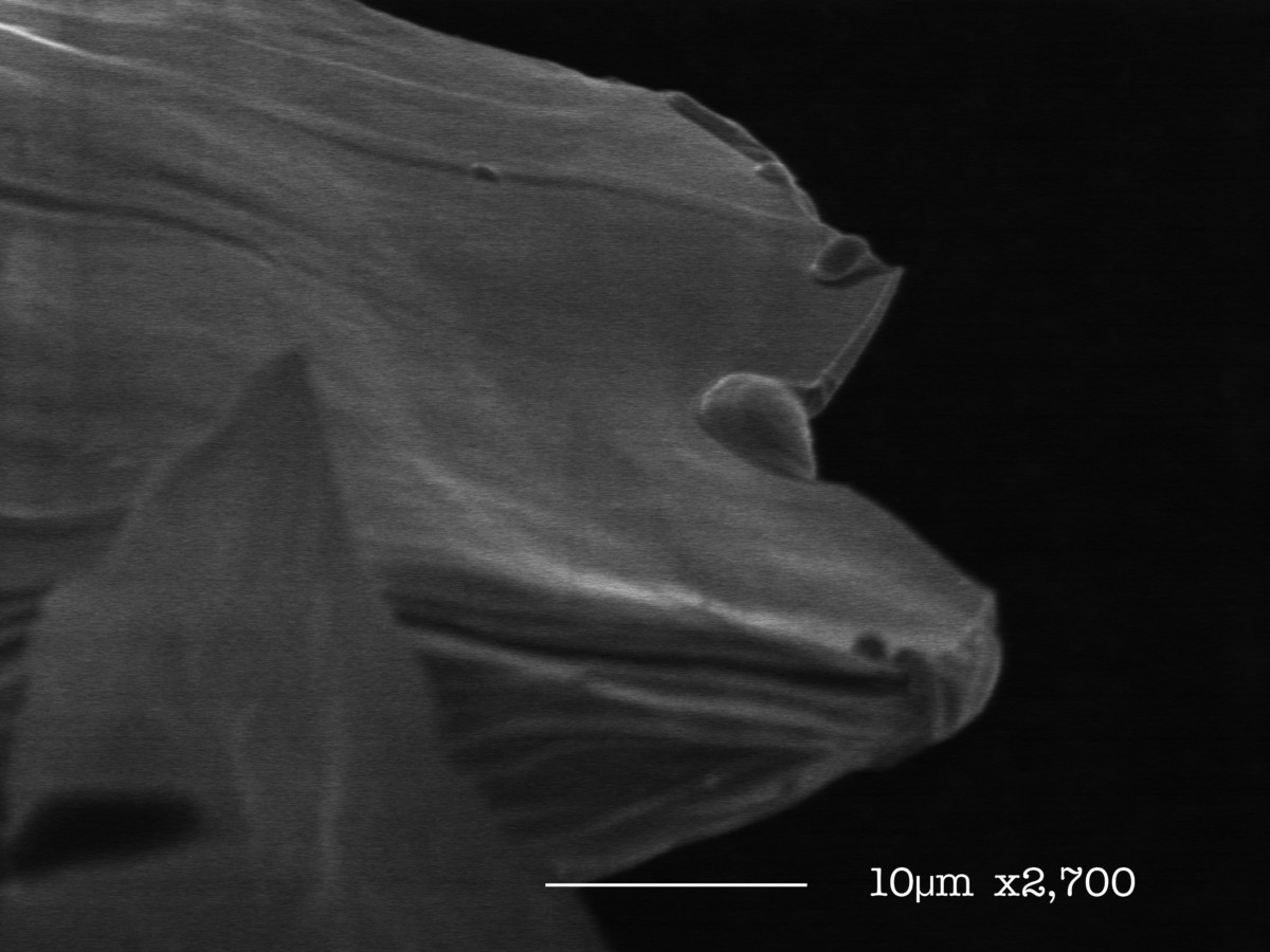
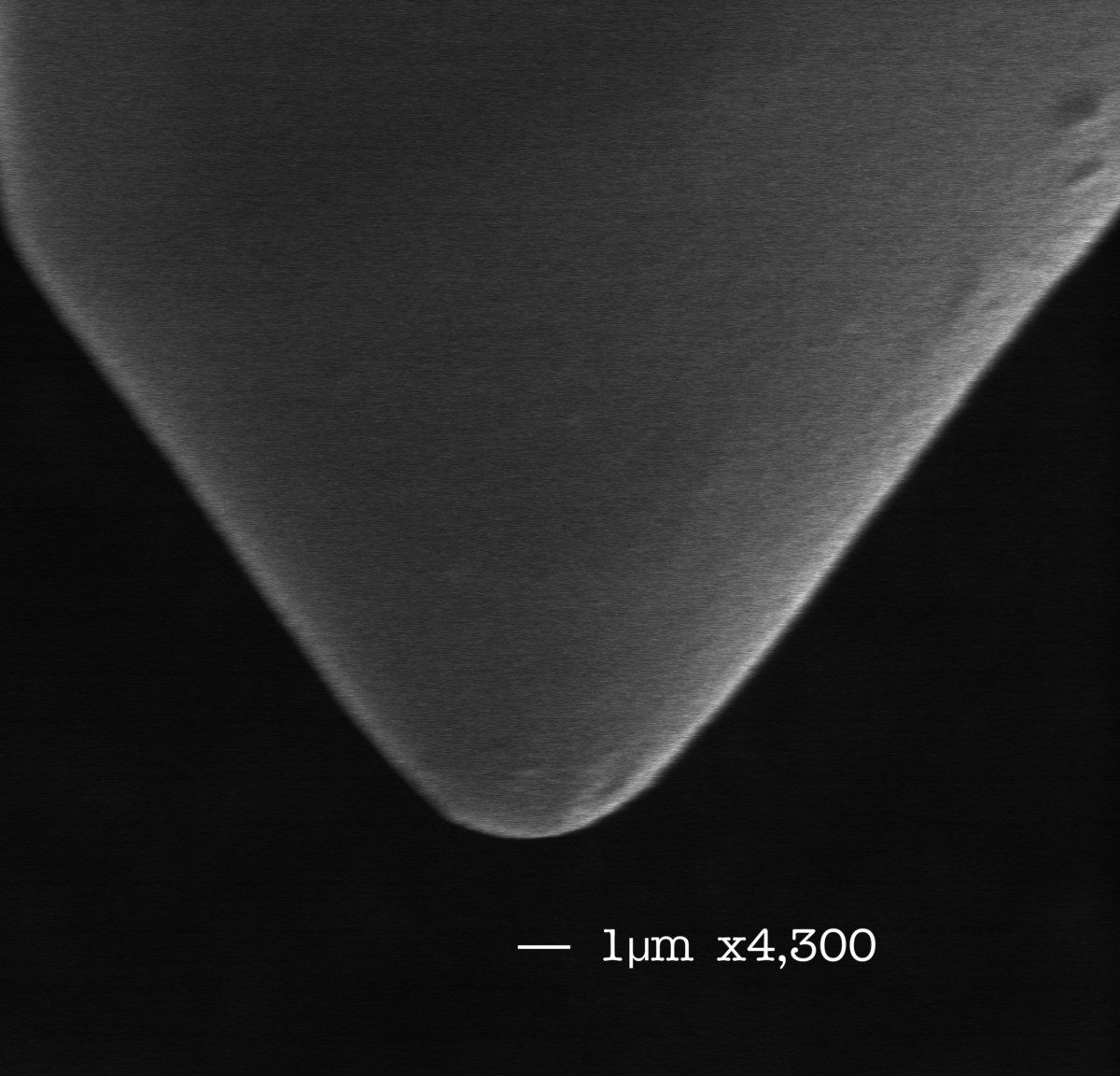
How small is small? Here’s an SEM image of the tip of a scalpel for scale.
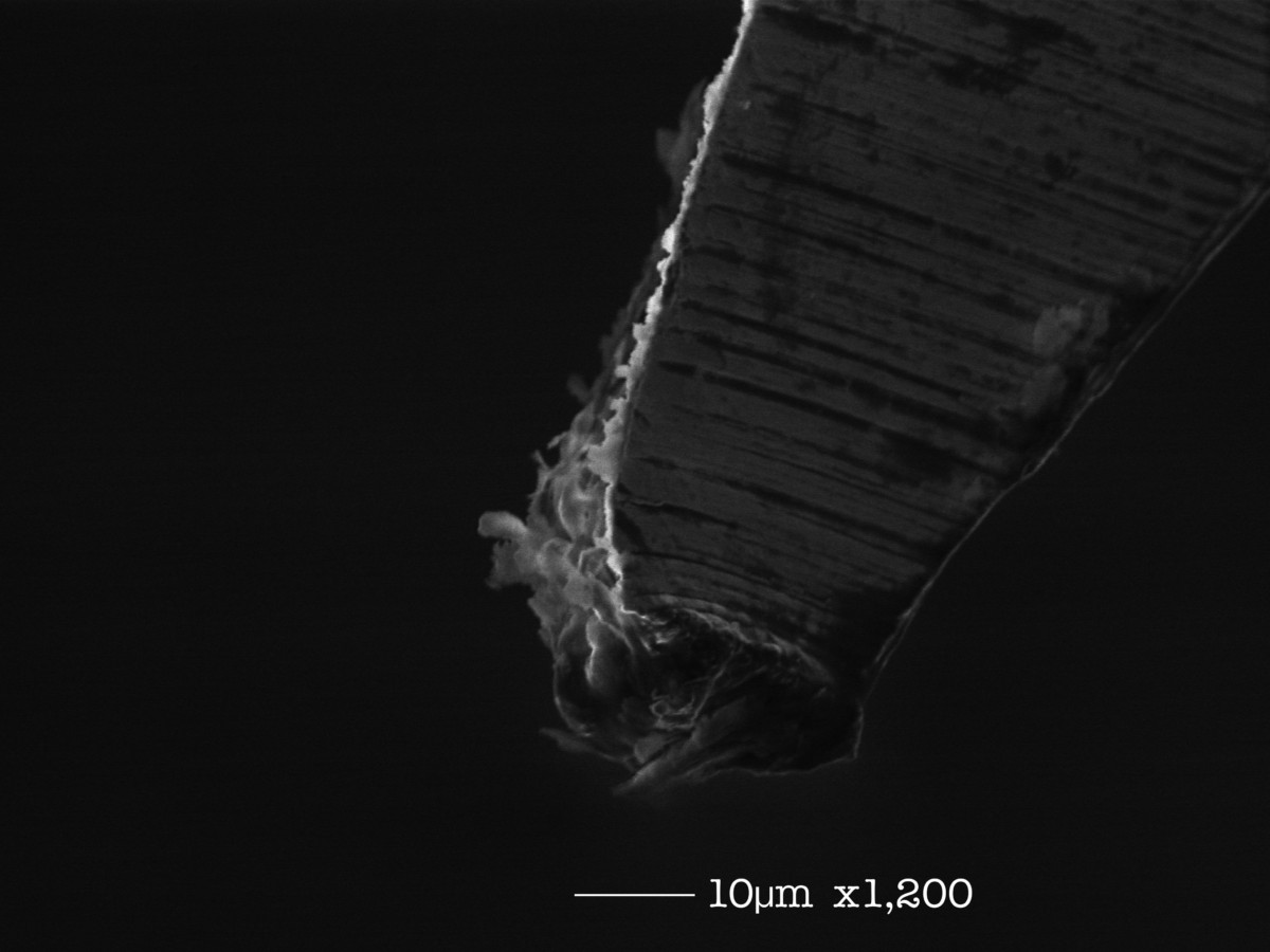
You can see that the tip is between 15 and 20 µm across. If you’re new to these units, µm is short for micrometer, or micron for short. A micron is one millionth of a meter, or 10-6 meters. That’s hard to visualize, so I think of 100 microns as about the smallest thing I can see with my naked eye without squinting. For me, that’s as small as it gets without needing the help of SCIENCE. So at 15-ish microns there’s no way I could see the tip of that scalpel.
And yet at this scale, it looks like a crudely sawed off two-by-four.
The tip of a cold cathode FEG emitter is smaller than that. A lot smaller. The best cold cathode emitters are just a couple of tungsten atoms wide. How wide is that?
Depending on how you measure, Tungsten has a diameter on the order of a couple of hundred picometers per atom. If the tip were two tungsten atoms across, let’s round up and say that it would be about 500pm, or half a nanometer wide.
A nanometer is one thousand times smaller than a micron. So it is roughly ten thousand times smaller than the tip of that scalpel. Or one hundred thousand times smaller than I can see without squinting.
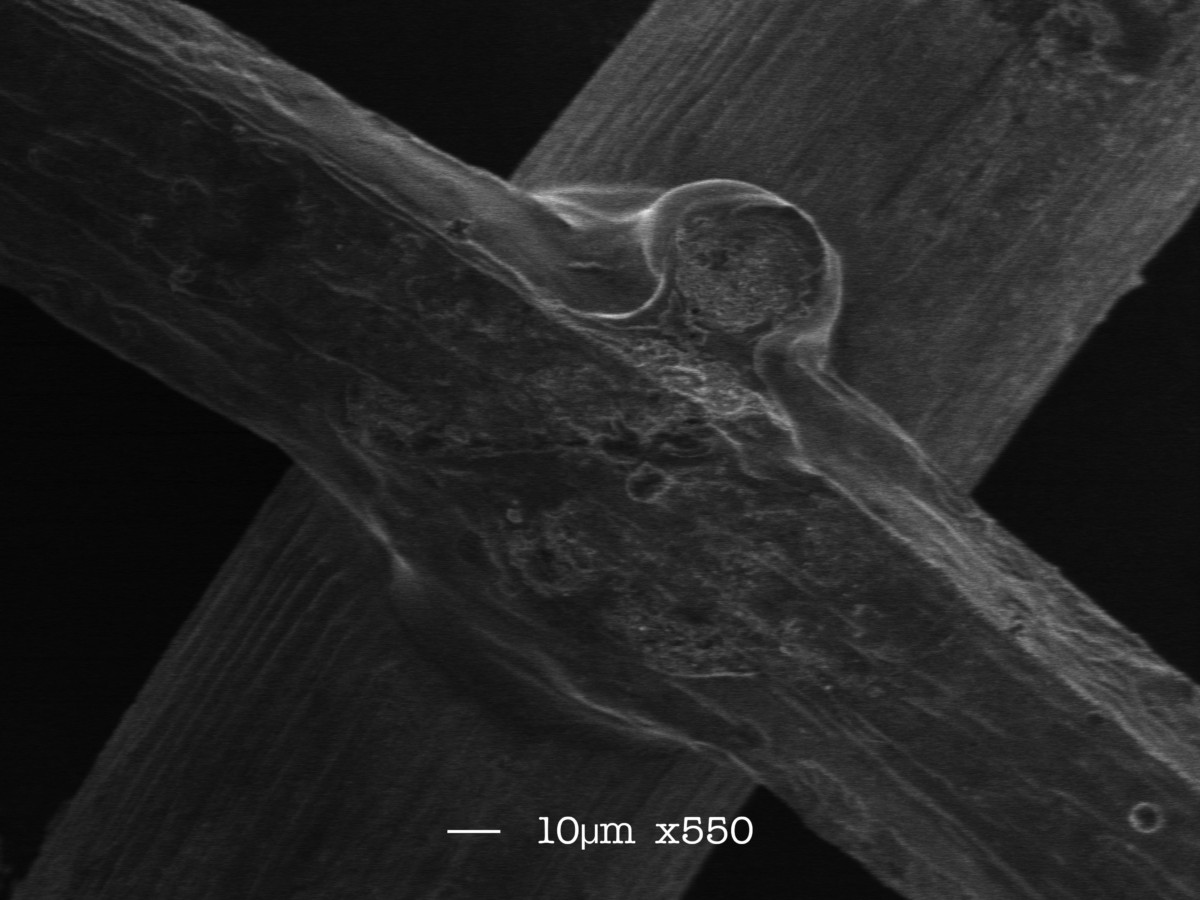
Let’s zoom into the original dead emitter:
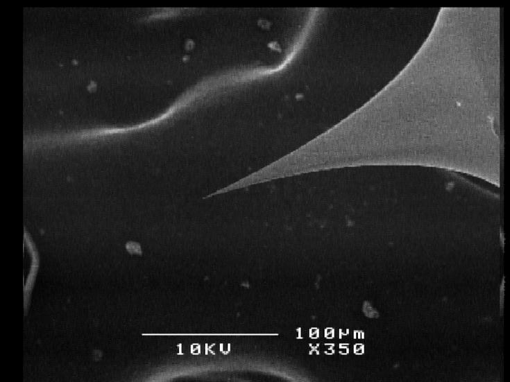
See the little bullfrog on the end of the tip? That’s why it died. Deformed through normal use. And bullfrogs belong on the dissecting table, not in your microscope.
Making a new emitter
The tungsten wire I use starts off as sintered polycrystalline wire about 100 µm thick. Like so much of what fills my shop, you can find it for relatively cheap on eBay.
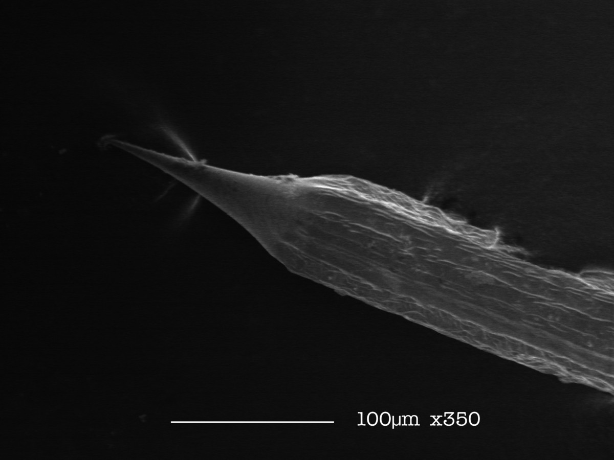
Here is what that wire looks like if you cut it with a sharp pair of wire cutters:
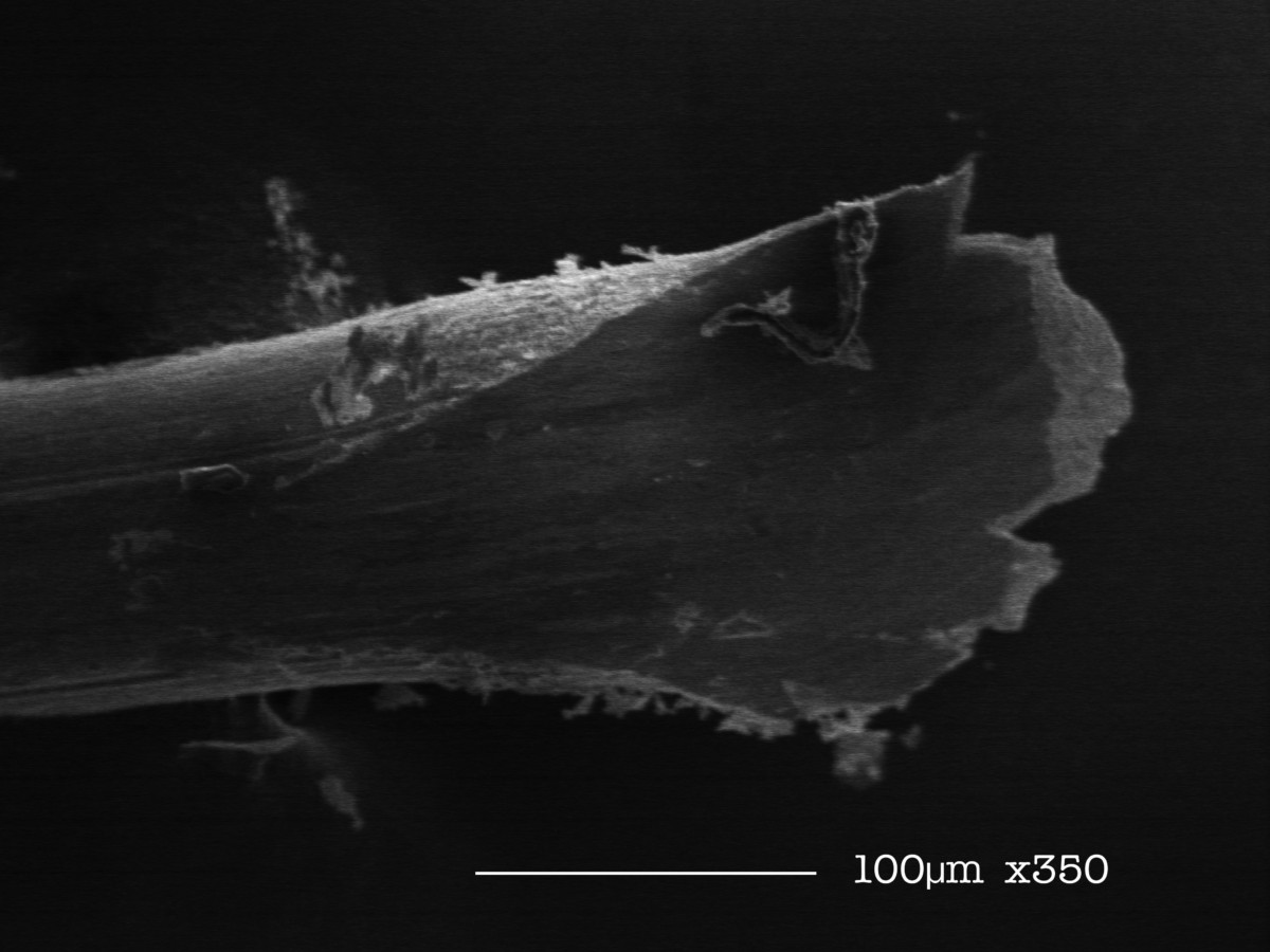
That white line at the bottom is for scale. It’s about as long as the wire is thick. The “x350” is the approximate zoom. You can see that cutting the wire makes it pinch and spread out. If I need to get the tip down to picometers, that clearly isn’t going to work.
Polycrystalline tungsten wire is tough stuff. The manufacturing process turns tungsten powder into a drawn wire with long, fibrous crystal structures. Electron emitter tips are made from monocrystalline tungsten, which is highly ordered and extremely brittle.
It might be possible to make a sharp tip by pulling polycrystalline wire until it breaks. Some people have reported success using this method for producing STM tips.
Here’s what a pulled polycrystalline wire looks like:
This wire is much, much sharper than the cut wire. But the end is a jagged surface made of those long fibrous crystals. It is still many orders of magnitude too wide to be used as an FEG.
Magic crystals
I’ve been attempting to recrystallize tungsten wire. The process involves hanging a weight on a loop of wire in a vacuum, and passing an electric current through it (like a light bulb). Over time the wire releases impurities and eventually melts and realigns. Here’s some tungsten stretching in my homemade vacuum chamber:
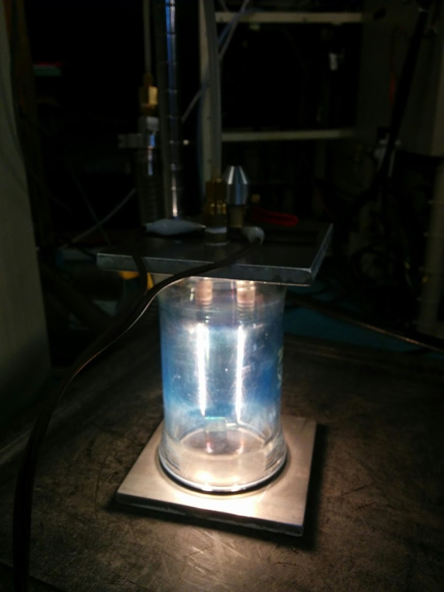
After stretching, the wire is extremely brittle. Handling it is difficult because it’s easy to break and hard to see! I lost half of my yield at one point by accidentally dropping a piece on the floor, never to be seen again.
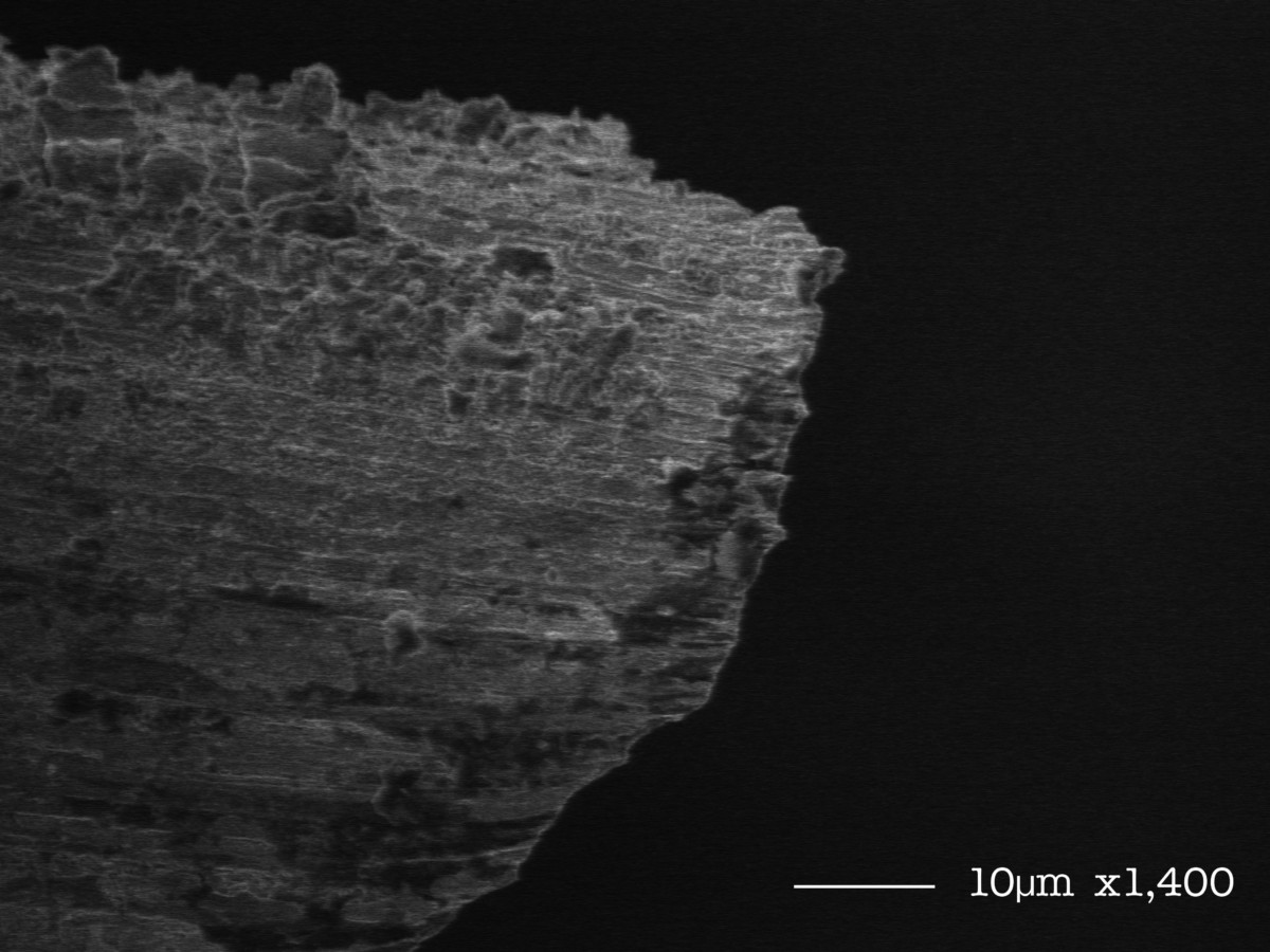
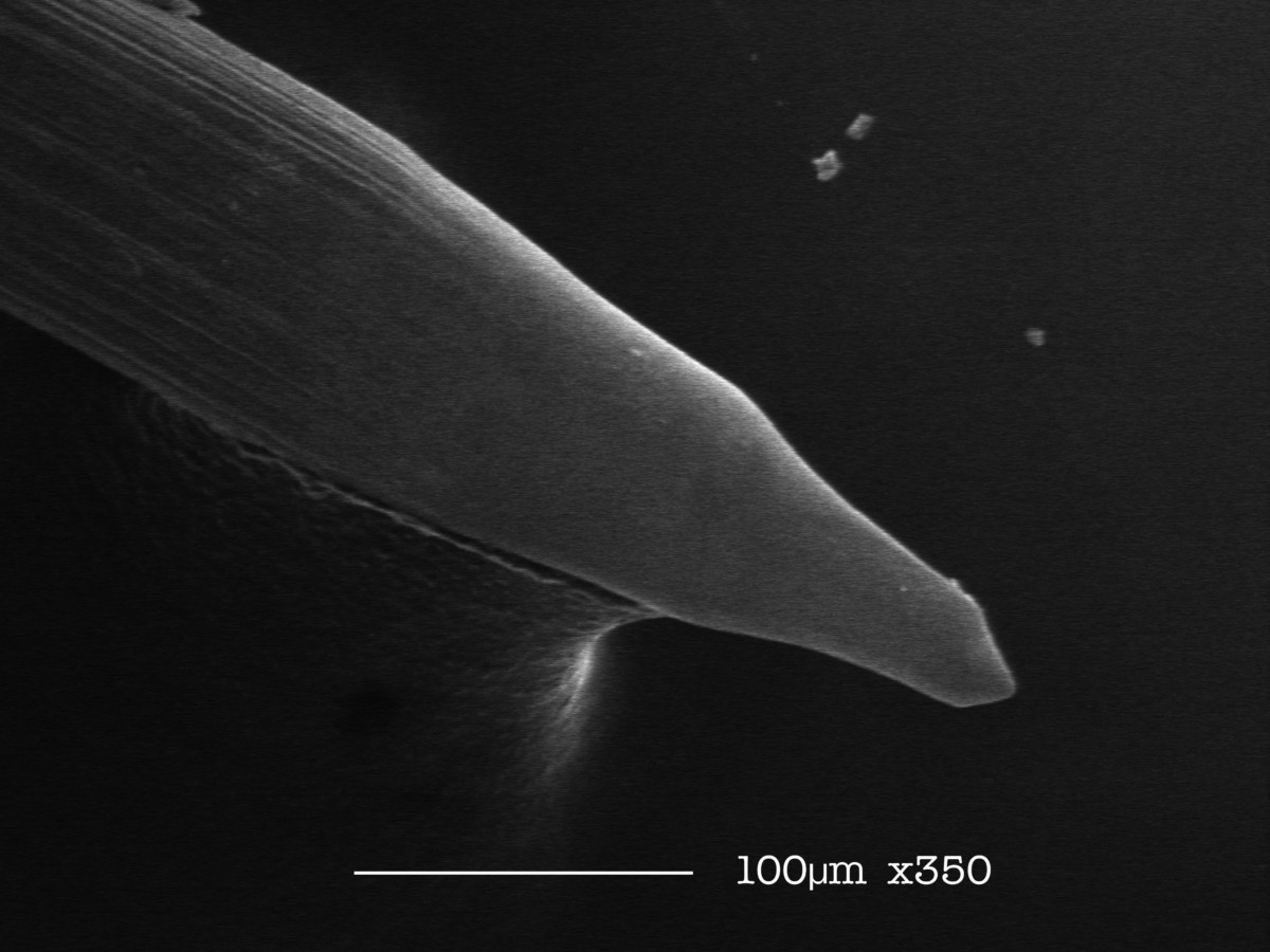
I wondered if the stretched and broken end of the filament might be sharp enough to use as a tip. Here’s what that looks like:
This looks much more promising. It’s still too wide to use as an emitter, but parts of that edge are less than 1µm thick. The smooth surface indicates a more ordered structure than those long random fibers.
In order to get the wire down to atomic scale, the tip needs to be electro-etched in lye. Clearly, anything with “electro” in the name means you need to pass electricity through it. But how do you affix a jumper clip to wire as thin as a human hair and as brittle as an egg shell?
I decided to spot weld some to a piece of polycrystalline wire, and grab that instead. Here’s one weld I made:
The recrystallized wire is on top. It’s thinner because some of it is now coating the inside of my vacuum chamber.
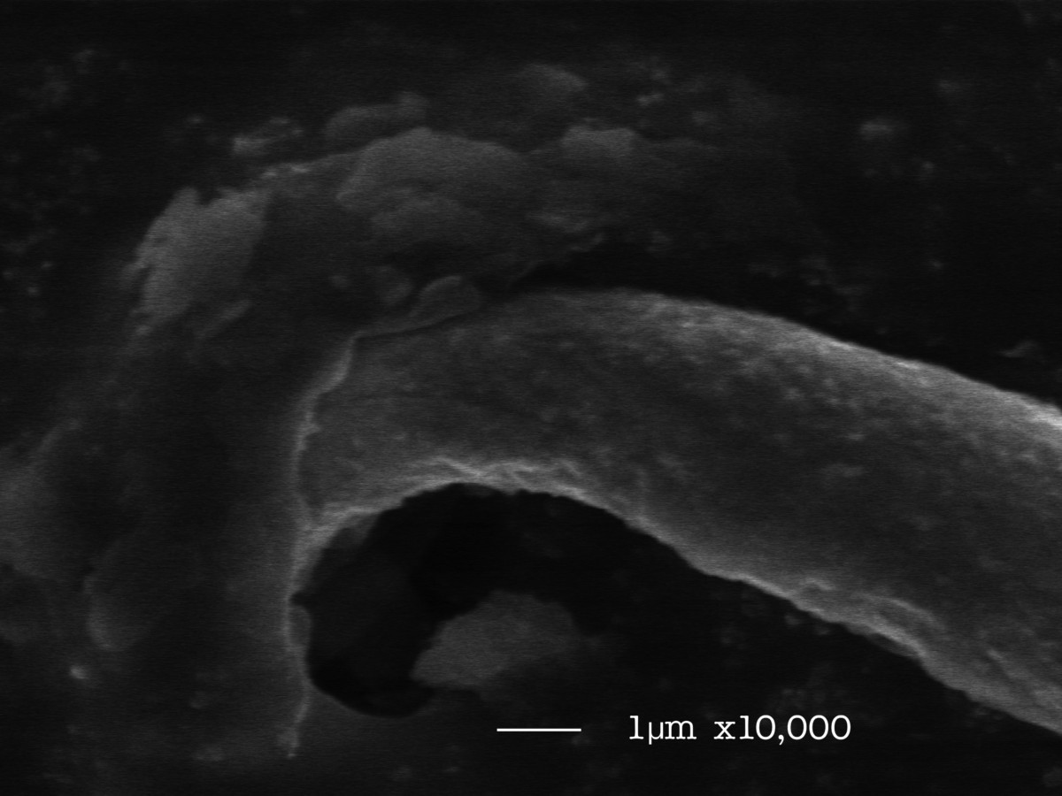
I made my first etch at 15V DC, and turned off the supply as soon as I saw the wire drop. This is the method that I used to make the emitter that took these pictures. Here is the first tip:
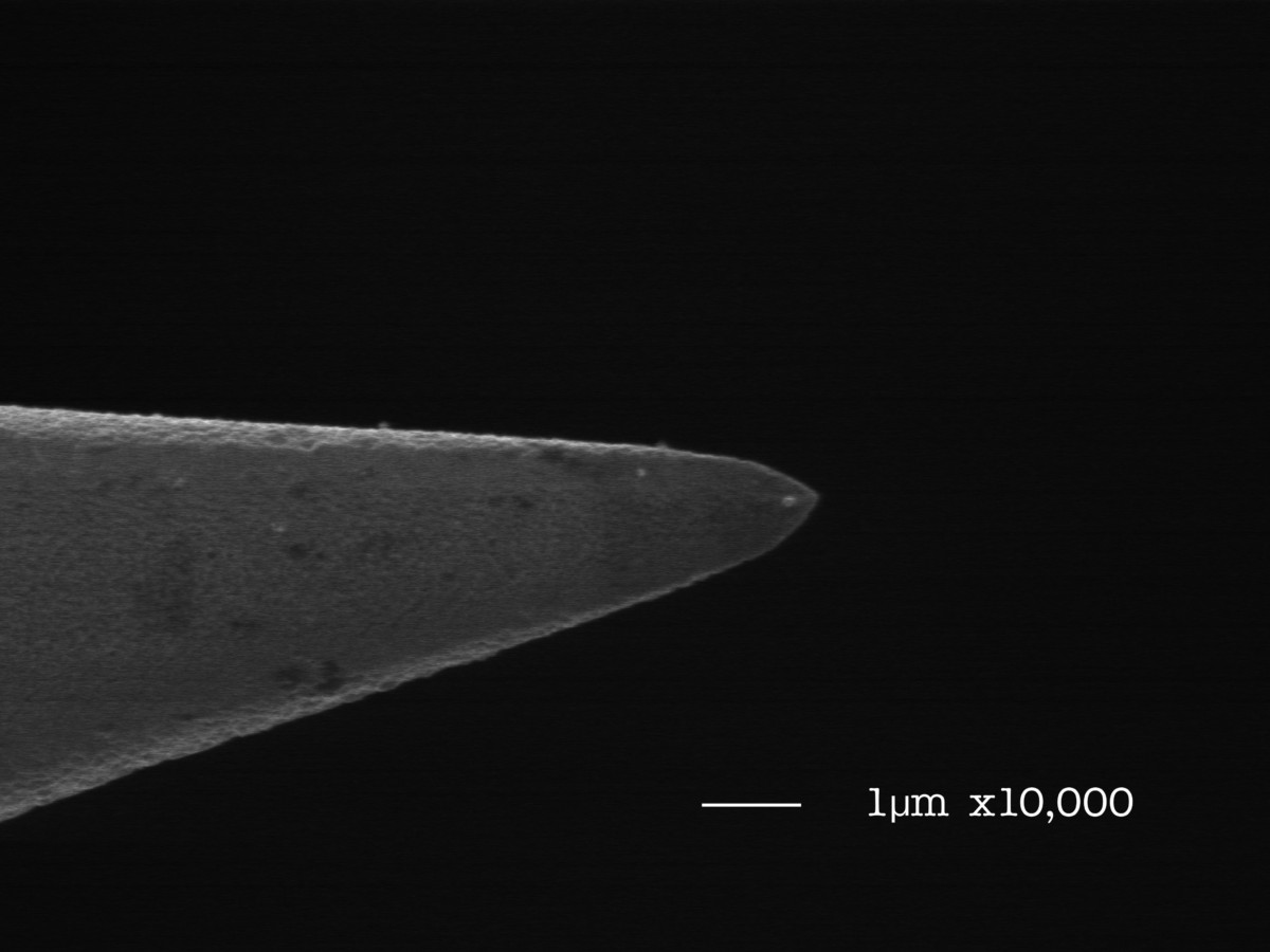
Not bad. Let’s enhance.
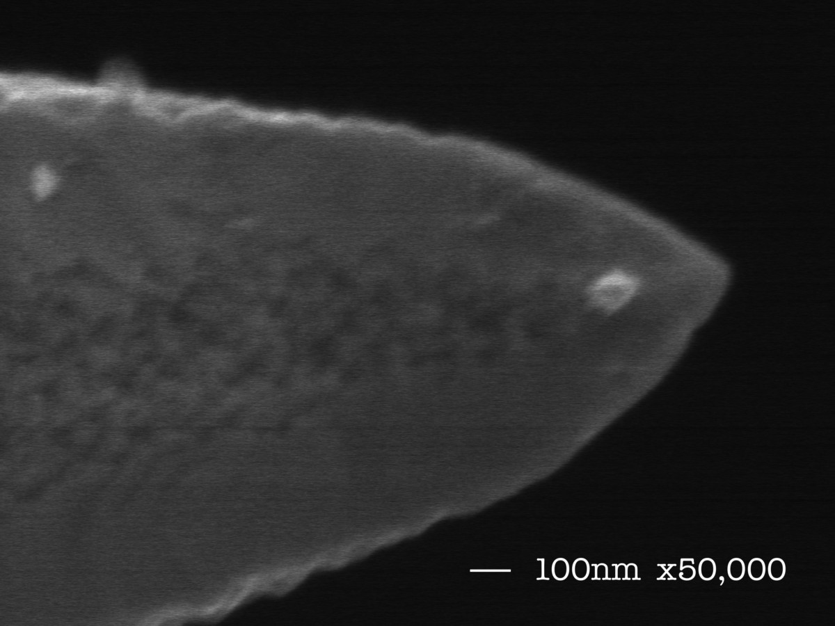
This is clearly better than any method so far. The result is a tapered tip about 20nm wide. Still 50x too big, but we’re getting closer! And considering that I took this picture with an emitter made the same way, this is clearly a viable method for making something functional, if not ideal.
I’ve read in various research papers that cutting off the electric flow more quickly after the etch results in sharper tips. I made a circuit based on a 555 timer (cribbed out of one of those papers) to detect when the etch has finished. It can turn off the current flow in a couple of hundred nanoseconds.
Here’s the first tip I made with that method:
Since it was the first time I used this circuit, I wasn’t sure what voltage to use or where to set the break sensitivity. I started at 15V, but after about five minutes it was clearly taking too long. I increased the voltage to 17V. The wire dropped almost immediately, but the sensitivity was set too low and the current stayed on. The place on the tip where the angle changes sharply is at the moment that I changed the voltage.
Since the current didn’t shut off immediately, it made a very rounded tip.
This tip is much too wide to use, but the etch was quite even. I had to try again.
The second try worked brilliantly. I etched at 17V, and the sensitivity was set just right. The wire dropped, and the current shut off. Boom!
Unfortunately, this was also the biggest disaster of the evening. After all that work, I somehow managed to stick the tip into the carbon tape while mounting it. The tip was totally destroyed.
If I can keep my clumsy human digits under control, I think I’m on the right track for making a proper emitter. The emitter I used to take all of these pictures is performing very well– the beam is more stable than it ever was with the original.
But I notice that I’m having a hard time getting below about x200,000. I’m not sure if the problem is with the emitter or with my basic SEM operator skills. I intend to make several more tips, and if I can get a reliable method down for making them much sharper, I’ll replace it. In the meantime I’ll post photos of interesting stuff as I find it.