New Year, New Emitter
The quest for an ideal light source
We can easily forgive a child who is afraid of the dark; the real tragedy of life is when men are afraid of the light. —Not Plato
What exactly is an electron emitter? Think of it as a very fancy light bulb, but for electrons instead of photons.
Traditional optical microscopes use light to illuminate a sample. Sunlight, LEDs, lasers, or any other source of light can be used. The light is reflected off the surface (or in the case of mostly transparent things, through the body) of whatever you want to examine. Lenses focus that light into an image that you can see with your naked eye or a camera.
The trouble with using light as an illumination source is that it moves as a wave. Even if your light source is completely uniform, and your optics are perfectly manufactured and aligned, the smallest features you can hope to resolve can be no smaller than about half the wavelength of the light you use. This is known as the diffraction limit. (Emerging techniques and materials may overcome this limit in certain circumstances, but this is a very active area of research and not likely to be something you’ve got on your bench just yet.) For imaging anything smaller than a couple of hundred nanometers, light simply becomes impractical.
Instead of using light, Scanning Electron Microscopes (SEMs) use electrons as an illumination source. Like light, electrons also have a wavelength that depends on how fast they are moving. The de Broglie wavelength can be calculated for any particle, and is directly related to its momentum. The momentum of electrons is quite tiny compared to light, so the corresponding wavelength is much smaller.
A smaller wavelength means more magnification (yay!) for more cost and complexity (boo!). An SEM uses an electron source instead of light, electromagnets instead of lenses, and a vacuum between the emitter and the sample to reduce electron scattering.
Keep in mind that the diffraction limit is just the ultimate restriction that physics imposes on us. Many other factors such as alignment, beam stability, and the beam size will limit your resolution long before you hit the diffraction limit.
Electron sources
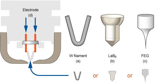
Many SEMs use a thermionic (heat driven) electron source. It works a bit like an old fashioned light bulb: heat up a piece of tungsten wire by passing an electric current through it, and electrons will spontaneously radiate. This produces an electron spot about 50μm wide.
Milly uses a Field Emission Gun (FEG) as an electron source. If a thermionic emitter is an electron “spot light”, the FEG is a laser beam: much brighter and tighter (0.01μm or smaller), yielding even better resolution imaging. It does this by using a tiny metal tip that can be as small as a couple of tungsten atoms thick.
So why don’t all SEMs use FEGs?
To sum it up in one word: cost. For a FEG to work at all, it needs to operate at Ultra High Vacuum (UHV), about 10-9 torr . This is about ten thousand times better vacuum than a thermionic emitter needs to function. This means copper seals, ion pumps, additional valves, and significantly greater cost and complexity.
I’m fortunate enough to have Milly, so the cost of the vacuum chamber and pumps isn’t an immediate problem. But that brings us to the other big cost difference between a cold cathode FEG emitter and a thermionic filament: how it’s made.
(Of course, there are many other engineering considerations and physical constraints beyond cost as well. See this presentation for a nice overview of the differences between various electron sources.)
Since Milly developed beam stability issues earlier this year, I began to suspect that her emitter might need replacing. I have been unable to find a reasonable source for a replacement, and equivalent Shottky sources seem to run in the neighborhood of ~$3k. This is quite a bit outside my fun budget, so I decided to try my hand at making one.
Magic crystals
While it’s possible to make a tip from sintered polycrystalline tungsten wire (i.e. the kind you find for cheap on eBay), it won’t be nearly as sharp as a tip made from a single crystal.
I found this entry on the Surface Science Network Wiki that suggests recrystallizing it by hanging a weight on the wire in a vacuum and passing a current through it. I did exactly that and ended up with very straight, very brittle tungsten.
I have no idea if it actually recrystallized, but I thought the process couldn’t hurt. I’ll make more of these tips and image them with Milly once she’s back online.
Welding Wolfram
It turns out that tungsten (wolfram) has the highest melting point of any element: over 3400C! It’s also notoriously brittle and just itching to combine with oxygen to make useless powdery oxides. But I needed to somehow make three spot welds to make the new emitter.
My first welding experiments were a total disaster. First I tried to use a benchtop power supply and lithium ion batteries to make the weld. Later I “upgraded” to a rewound microwave oven transformer.
But while this provided plenty of power, the rise time of the current was far too slow. Instead of a good weld, I got broken wire.
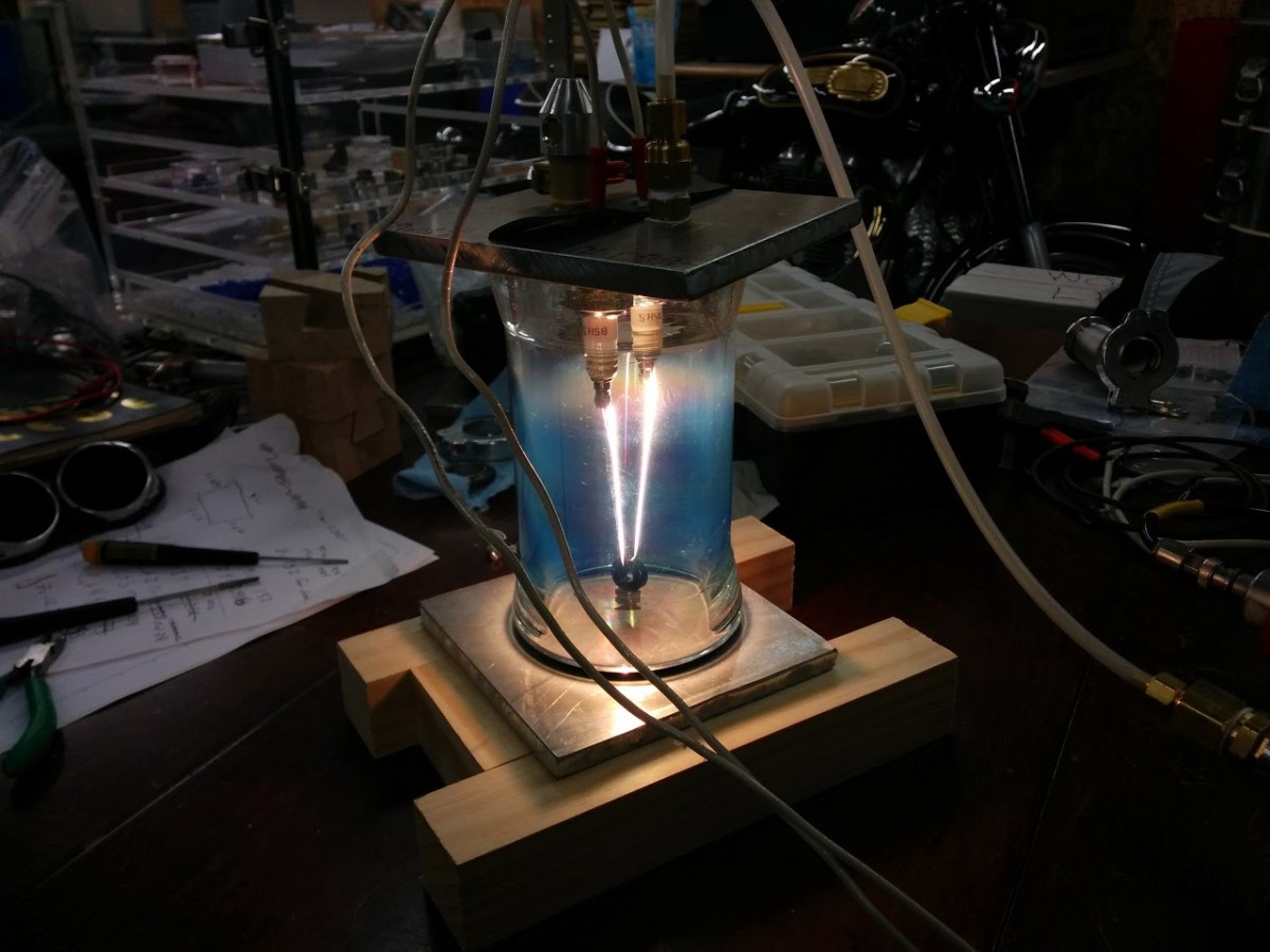
I later realized that what I needed was a capacitive discharge (CD) welder. The only trouble being that they cost about as much as a replacement emitter. While I could probably design and make one, I realized that the current drone craze has made custom lithium ion battery pack manufacture a thing. And you need a CD welder to get the tabs affixed to the individual battery cells.
One quick eBay stop later and I found this $100 beauty.
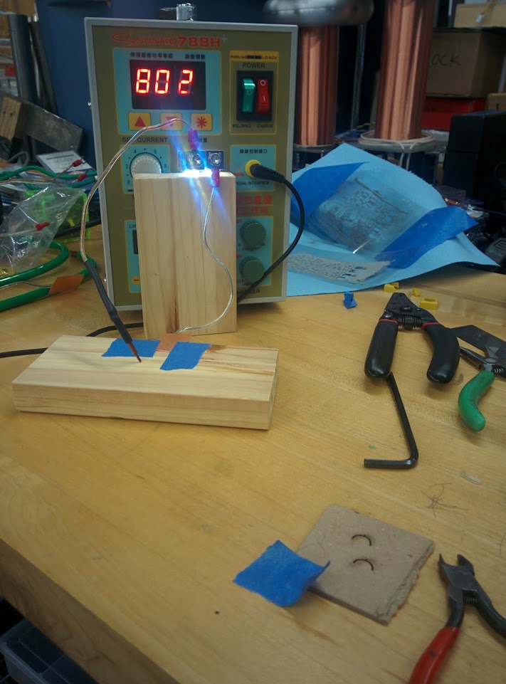
Sure it trips the breaker as soon as I plug it in, and I had to disassemble it and add insulation to keep it from burning down the shop, but what a deal! A couple of quick mods later, and I was in business.
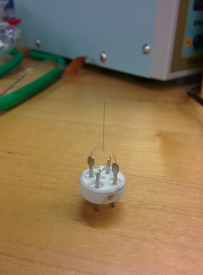
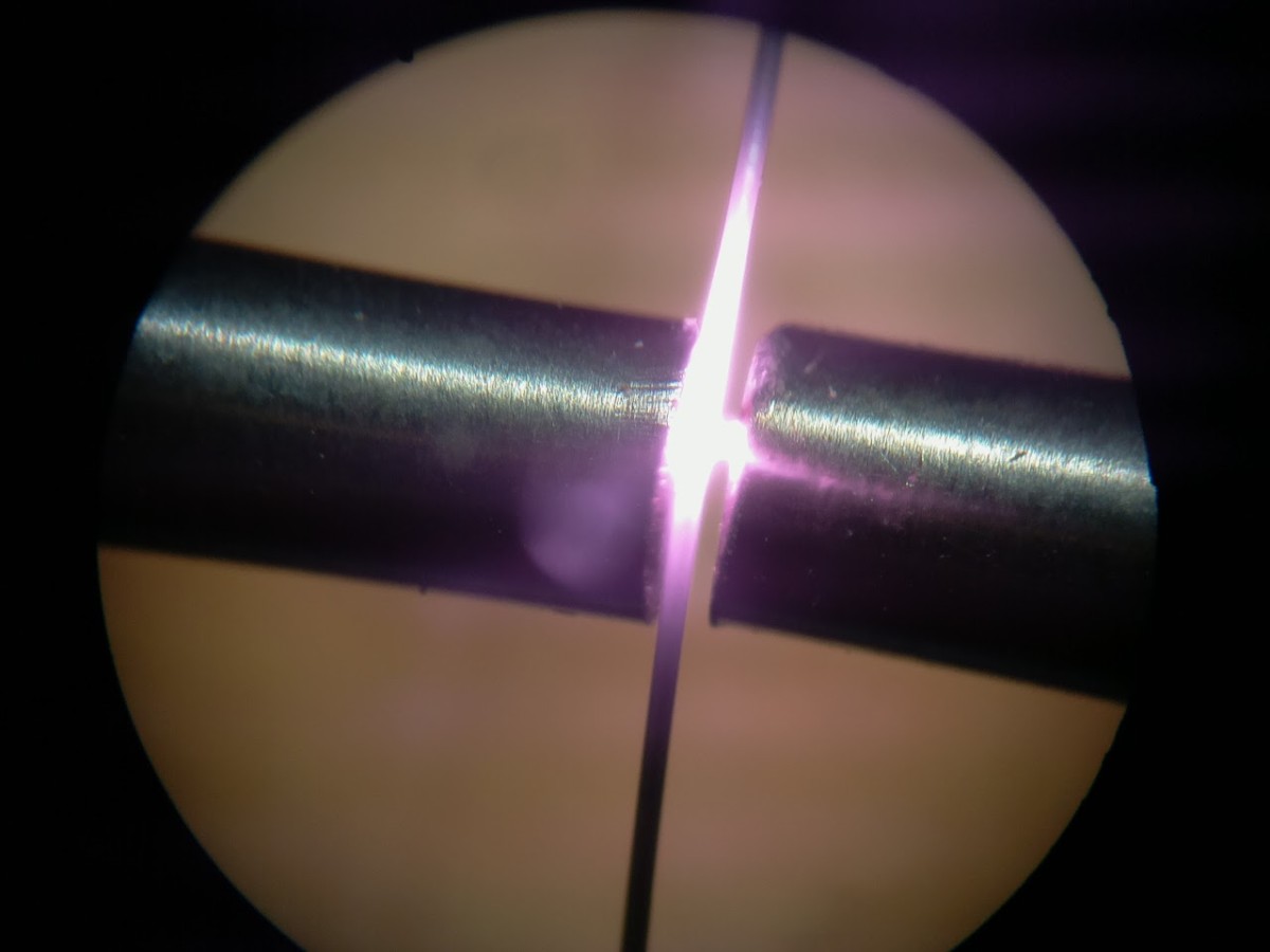
Rather than spot weld a new arc onto the emitter pins, I removed the old tip from the existing wire with tweezers. Then I welded my monocrystalline wire to the arc. I saved the old tip so I can look at it under the SEM later (assuming this crazy experiment works, of course).
Get to the point
Okay, so I can stick arbitrary pieces of tungsten wire to each other. And I might have a magic wolfram monocrystal. But how do you even go about making something atomically small?
The tungsten wire itself is only 0.1mm thick (and tiny yet tough enough to pierce your finger like a hypodermic needle if you’re not careful). But that is still roughly a million times too wide.
Filing it down on the belt sander clearly isn’t going to cut it.
After quite a bit of online research, I found this excellent 2004 thesis by Anne-Sophie Lucier, “Preparation and Characterization of Tungsten Tips Suitable for Molecular Electronics Studies“ (pdf). It’s well written and approachable by junior scientists like myself. Most importantly it is not locked away behind a paywall like every other relevant research paper I could find.
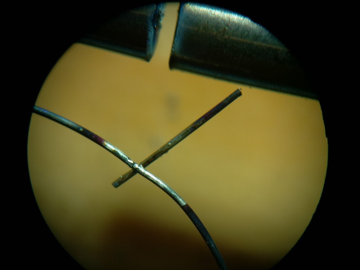
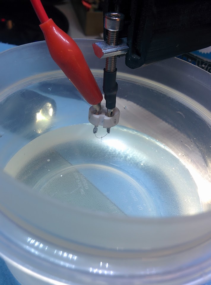
The basic idea is to electroetch the tungsten wire in a sodium hydroxide (lye) solution. You pass an electric current through the wire and solution, and it preferentially etches at the meniscus. When the wire finally breaks, the resulting tip is extremely sharp– if you’re using monocrystalline wire, it may be just a few tungsten atoms wide.
Here’s the rig I came up with. The screw let me finely adjust the height of the wire in the solution. I used a piece of carbon as the cathode and etched it for several minutes at about 7V.
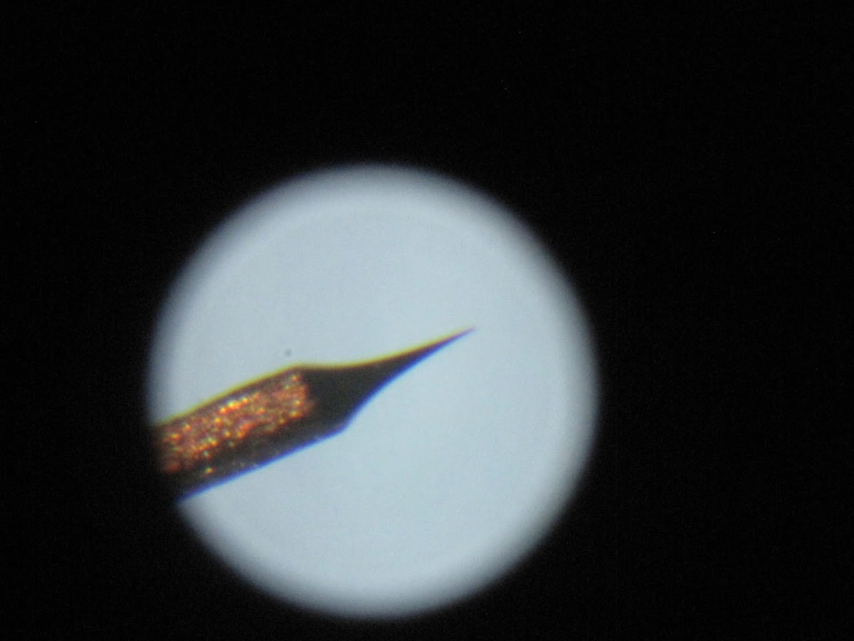
The resulting tip was maddeningly sharp. Here’s one I made at ~20x magnification.
Line it all up
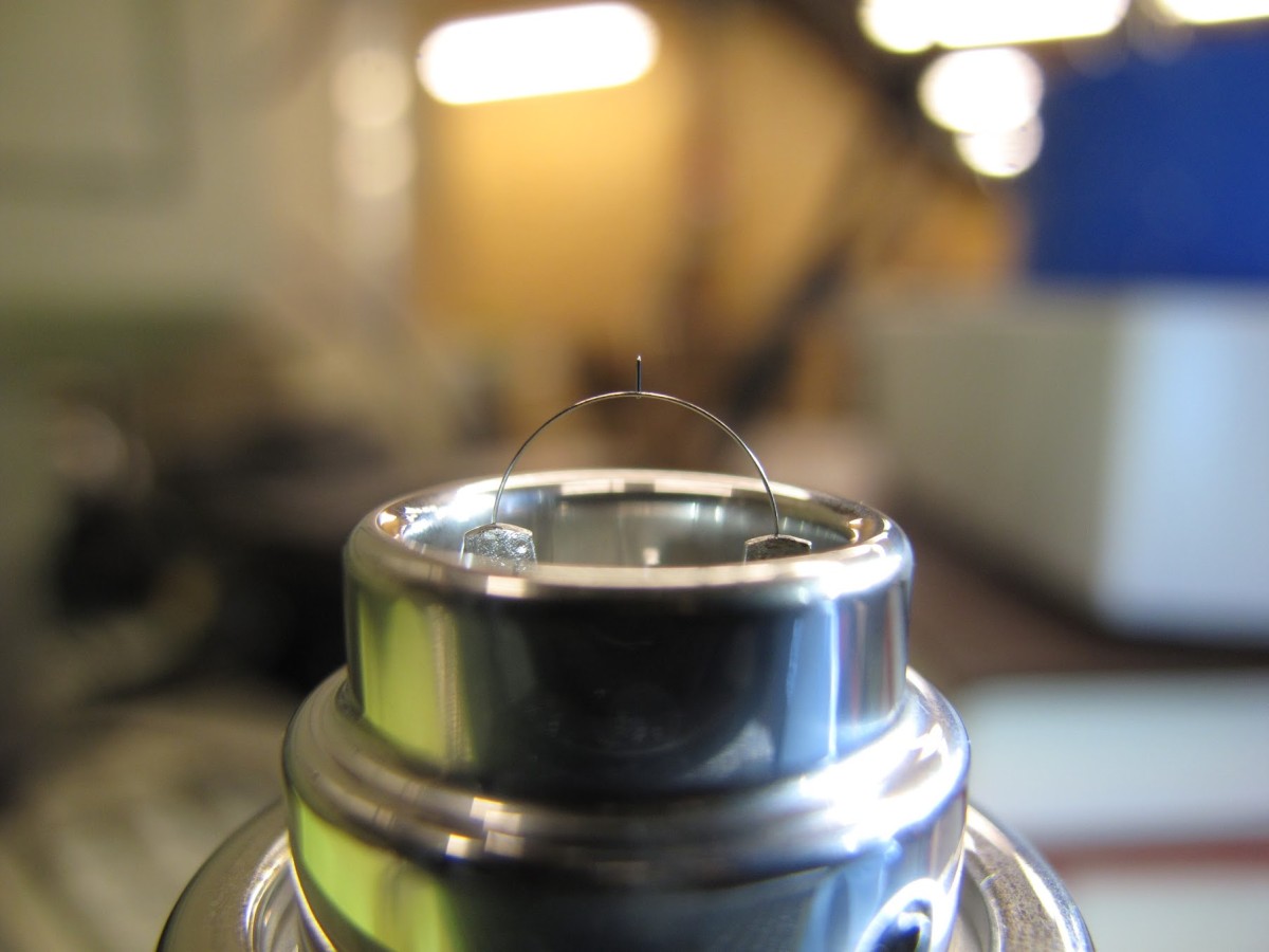
With the emitter ready to go, I next needed to make sure that it was properly aligned with the extraction anode. The emitter itself sits inside of a large assembly of porcelain, gold, and various highly polished metals. I set the module up under the optical scope like this:
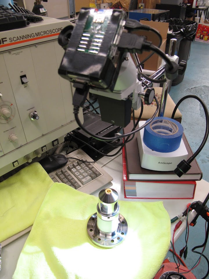
The extraction anode itself is a tiny gold disc. By carefully aligning the optical scope with the hole in the anode, I could just see the tip of the emitter peeking through.
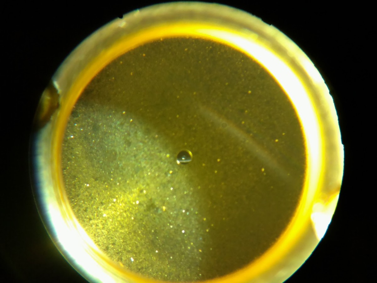
By adjusting the set screws on either side of the anode housing, I got the emitter tip perfectly (I hope!) aligned with the hole.
Yes, but did it work??!?
I’m not sure yet. Now that everything is reassembled, and a fresh copper seal is installed, I need to get the vacuum back down to 10-9 torr. This process is… involved.
The last time I brought the column to atmospheric pressure it took a 30-hour bakeout procedure to get it back down. I’ve been baking the column all day, and I hope to get it back online tomorrow after it cools.
So until next time, may the New Year bring us peace, hope, deep vacuum pressure and stable beam emissions!